


The 27th
Printed Wiring Board EXPO
PWB 2026
Dates: January 21 (Wed) - 23 (Fri), 2026, 10:00 AM - 5:00 PM
Venue: Tokyo Big Sight
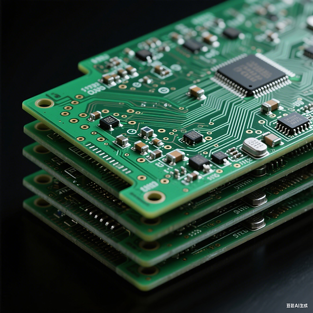
What is Printed Wiring Board EXPO?
A specialized exhibition where the world's most advanced printed wiring boards are exhibited in
one place
Previous venue scene
The latest printed wiring boards and related technologies that support the improvement of functionality and performance of electronic equipment will be exhibited.
It is an excellent place to conduct business negotiations and technical consultations with engineers in electronic devices, smartphones, automotive electronics, etc.
Including this exhibition, it will be held in Nepcon Japan, which consists of the following exhibitions.


Held annually
Concurrent Exhibitions

Advisory Committee
We have the cooperation of the following people who are active on the front lines of this field.

Yutaka Iinaga
Director,
Design Center
, OKI Circuit Technology Co., Ltd.
Yuki Hirokawa
Panasonic Industry Corporation,
Electronic Materials Division,
Electronic Substrate Business Unit,
Product Development Department, Development Division 1, Manager
Hirofumi Matsumoto
President and CEO of Flexlink
Technology Co., Ltd
.
Mitsuaki Toda
Meiko Co., Ltd.
Cooperative Design and Development Office Manager
Tsukuda Tatsuaki
Renesas Electronics Co., Ltd.
Senior Manager,
Package Design Engineering,
Package Design & Simulation,
Global Packaging & Assembly Division,
Operations Group
Minoru Kakiya
Team Leader,
Elemental Technology Development Team
,
Laminated Materials Development Department,
Development Center, Electronics Business Division, Resonac
Corporation

Service Units Japan Ariake Co., Ltd..
ADRESS 104-0061
Ginzaitchōme 22-ban 11-gō Ginza Ōtake bijidensu 2 F Chūgoku
E-MAIL: ariakejp1@gmail.com
http://www.ariakejp.com
Priority is given to email contact
VIP Members Club
post code:104-0061
ADRESS : 22-ban 11-gō Ginza Ōtake bijidensu2F
E-MAIL: ariakejp1@gmail.com
http://www.ariakejp.com